Authors: Artem Rodichkin, Anna Evseeva, Polina Maslova, Inna Mironova, Semen Archipov, Chechulin Michail
Developed in a school design bureau - part of scientific and engineering educational cluster of a laboratory for continuous mathematical education
Logistor logic
A method of radical performance increase of semiconductor computing devices based on:
In chips, mathematical operations are described by logic circuits, that are represented by a series connection of CMOS transistor assemblies
Mathematical operation execution time is determined by the sum of each series-connected transistor assembly execution times
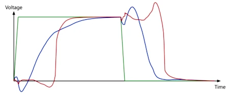
To demonstrate the delays when connecting logic elements in series, a circuit assembled in LTSpice is presented, which shows 4 series-connected CMOS inverters (spice models of real 10nm FinFET transistors are used)
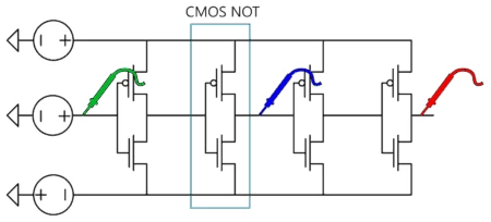
In the graph below, you can see the initial pulse (green) and signal delays that occur when 2 (blue) and 4 (red) inverters
We propose new type of transistor - "logistor", which is a transistor with output signal isolated from control signal. Logistors can also be used to replace optocouplers
The following interactive simulation (drag to intaract) demonstrates how conducting channel is formed and destroyed when voltage between Gate and Base is applied. Drag down to increase Gate-Base voltage; Drag right to increase Source-Drain voltage
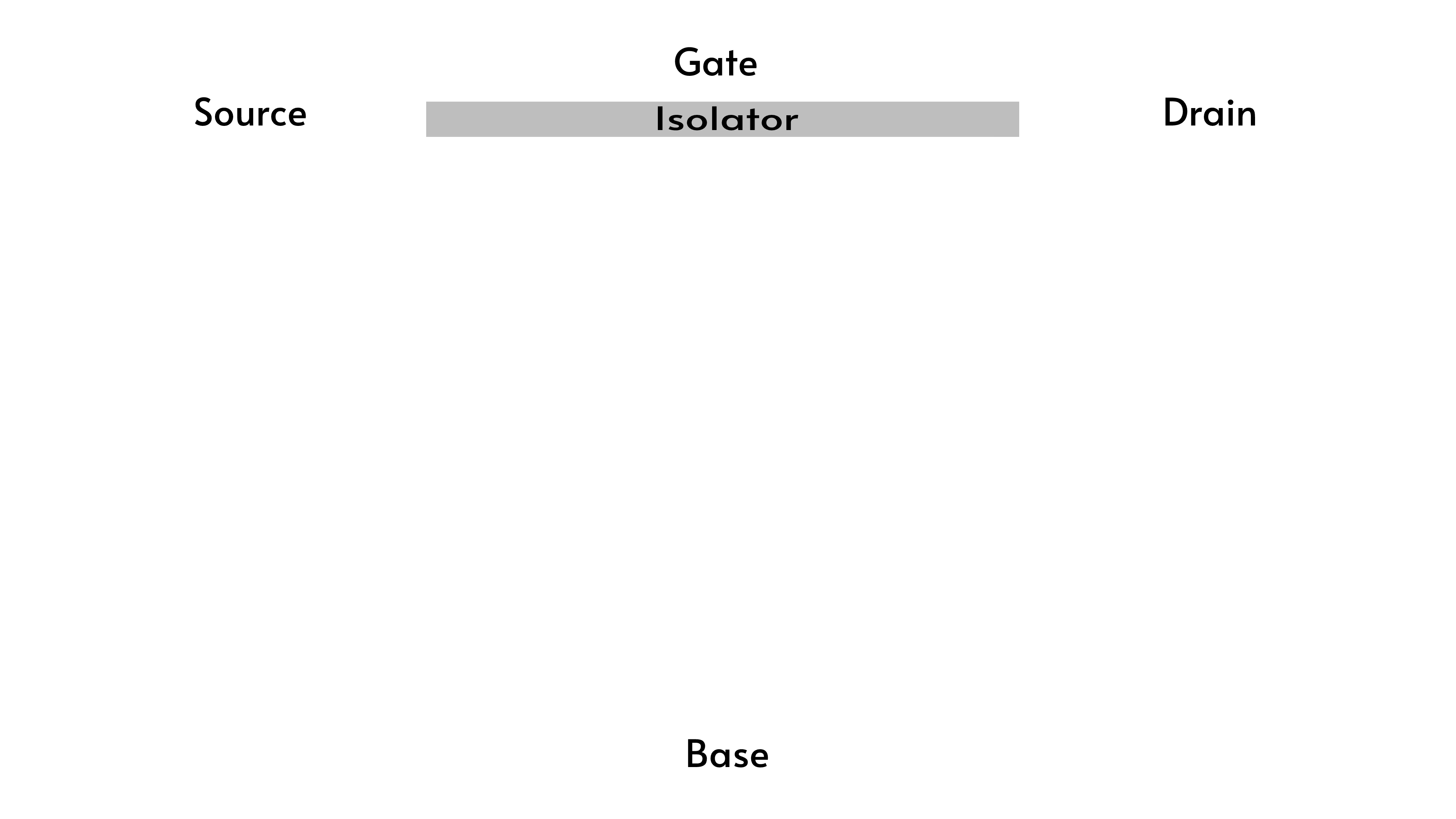
It has 4 terminals - Source, Drain, Gate and Base. When sufficient voltage is applied between Gate (+) and Base (-), negative charge carriers accumulate between Source and Drain and logistor starts conducting. If sufficient negative voltage is applied between Gate and Base, Logistor stops conducting
Volt-ampere characteristic of a logistor
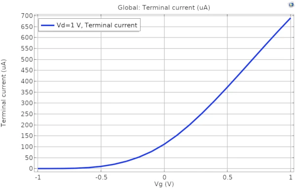
Unlike NMOS and PMOS transistors, used in CMOS, Logistors may conduct if no voltage is applied between Gate and Base. That allows different doling profiles which leads to approximately 3 times higher allowed currents between Source and Drain, according to Comsol simulaion, which in turn leads to performance gains
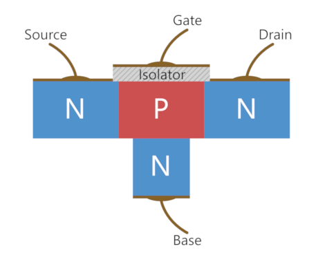
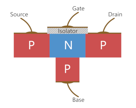
Transistor types that can be used in logistor logic:
NMOS PMOS
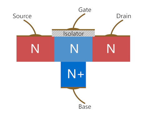
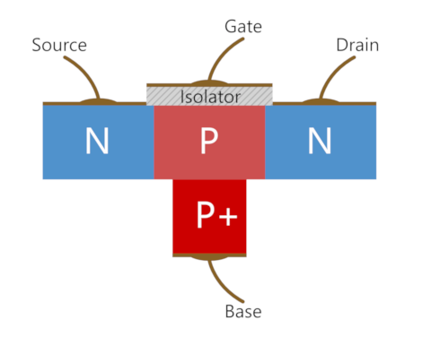
N channel logistor (NLOG) P channel logistor (PLOG)
Logistor logic input requires, "0" and "1" to be encoded the following way:
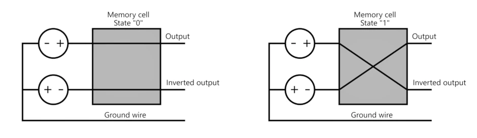
Each memory cell has 2 outputs - "output" and "inverted output". Output signal is the voltage between output and ground. Logistor logic requires two power supplies
Logistor circuits
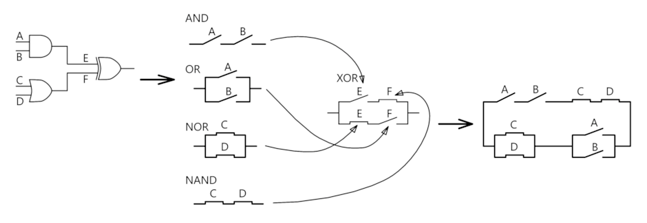
Logistor circuits are different from TTL, CMOS, and other methods of connecting transistors. "To gate" operations are not allowed in logistor logic with unlimited parallelism factor (number of gates controlled by single logistor). The following image describes concept of how logistor circuits should be designed:
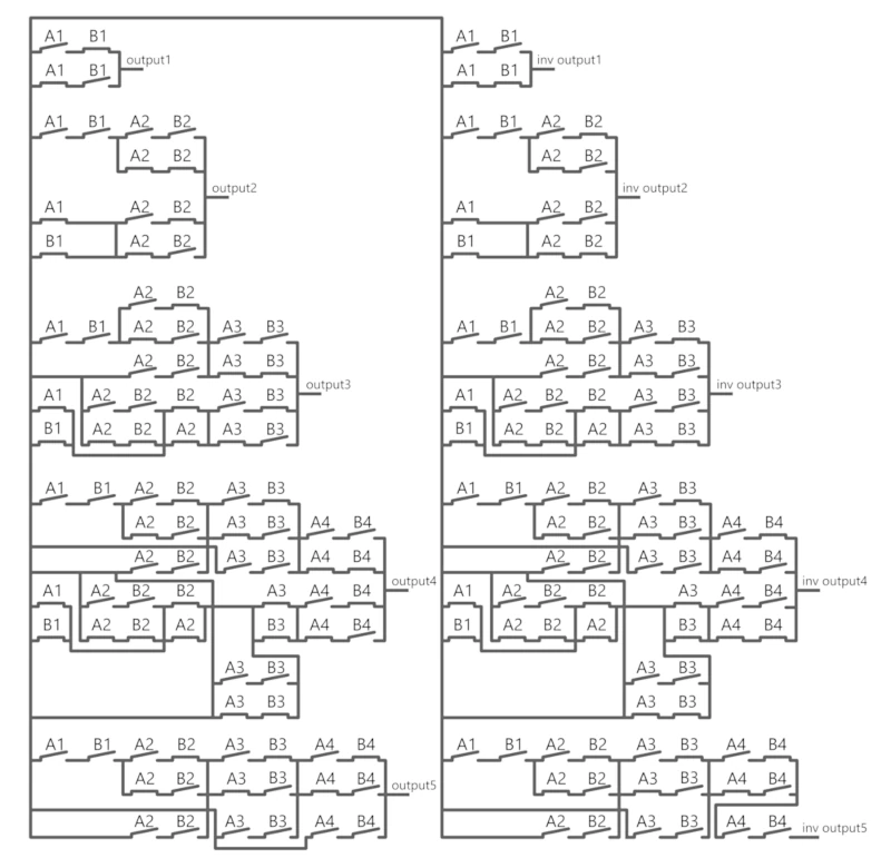
Logistor based adder of two 4-bit numbers
A1, A2, A3, A4; B1, B2, B3, B4 - first and second 4-bit number
Outputs - the sum of A and B
Inverted inputs are represented by switches in conducting state, while non-inverted inputs are represented by switches in non-conducting state
ALU based on logistor circuits output may or may not match input "0" and "1" input format, thus may or may not require “normal” and a complementary logistor circuits
If the non-complementary circuit outputs 0, then the complementary circuit outputs 1 for the same values at the inputs
Simulation of a 4-bit adder in Logisim (without the complementary part):
Top right - adder circuit
Bottom right - adder circuit where each output bit has an independent circuit (required for logistor logic with unlimited parallelism factor)
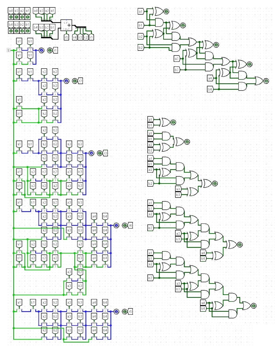
Press "reset" to start simulation; Click on white switches to change inputs
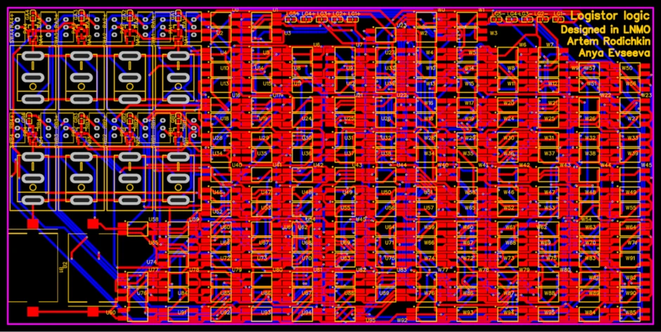
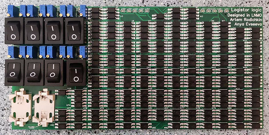
To confirm the operability of the logistor logic, a 4-bit adder circuit board was produced and it works
We designed electronic circuit in EasyEDA where optocouplers were used as a replacement for logistors (optocouplers are not logistors, but in this case they are suitable for concept demonstration)
To achieve high density of logistors (up to 225 MTr/mm2 for 32nm process), grid array with vertical and horizontal arrangement of gates (top view) is recomended. Single base contact should be on the bottom of substrate
Logistor logic with limited parallelism factor does not require each output to have an independent ligic curcuit. To achieve high performance, parallelism factor (~4) must be taken into concideration. Article presents only logistor logic with unlimited parallelism factor. No further documentation on that, sorry, you will have to figure that out yourself